Glass substrates for advanced packaging? Intel is on it
The US chip giant made a significant breakthrough in advanced packaging—and it’s all about glass substrate.
- The US chip giant has made a significant breakthrough in advanced packaging—and it’s all about glass substrate.
- Intel is expected to deliver complete glass substrate solutions to the market in the second half of this decade.
- That should allow the industry to continue advancing Moore’s Law beyond 2030.
In December 2022, Intel announced that its researchers foresaw a way to make chips ten times more dense through advanced packaging and a layer of a material just three atoms thick. The progress could pave the way to putting a trillion transistors on a chip package by 2030 – Intel’s most ambitious goal to date.

But Moore’s Law is supposed to be dead, and chips aren’t supposed to progress any further, at least not through traditional manufacturing advances. But Intel dismissed that notion on the 75th anniversary of the invention of the transistor in 2022. The chip giant said it could address the world’s increasing demand for computing and more effectively innovate to advance at a Moore’s Law pace.
This week, Intel unveiled that the answer for the next generation of semiconductors lies in glass substrates. “By the end of the decade, the semiconductor industry will likely reach its limits on being able to scale transistors on a silicon package using organic materials, which use more power and include limitations like shrinkage and warping,” Intel said when announcing its breakthrough innovation for its next-generation of advanced packaging.
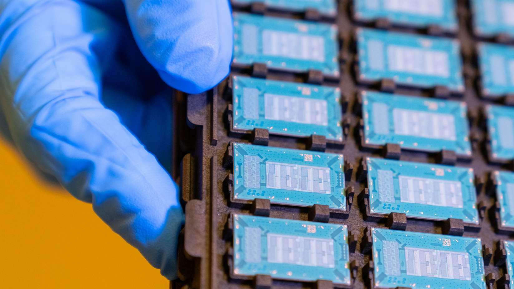
Glass substrate test units at Intel’s Assembly and Test Technology Development factories in Chandler, Arizona, in July 2023. (Credit: Intel Corporation)
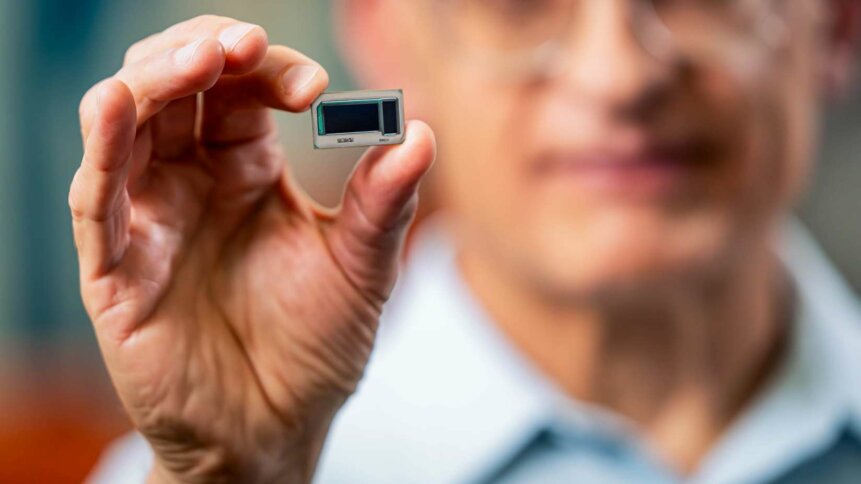
Emphasizing that scaling remains crucial to the progress and evolution of the semiconductor industry, Intel announced that it has begun a years-long transition to new technology that rests processors on a bed of glass instead of today’s epoxy-like organic resin. The new glass foundation, called a substrate, offers the speed, power, and real estate necessary for the chip industry’s shift to new technology, packaging multiple “chiplets” into a single larger processor.
What is advanced packaging?
Advanced packaging helps meet the demand for semiconductors that run emerging, mainstream applications—especially artificial intelligence (AI). These applications require high-performance, low-power chips that rapidly process massive amounts of data.
Advanced packagin to re-ignite Moore-s Law progression?
Despite the prediction by Intel co-founder Gordon Moore, who 1965 posited that the number of transistors on a microchip would double every couple of years, node advancement is now reaching its limits. As a result, technical advances on the front end of chip manufacturing are slowing, and the economically viable maximum size of a die, and thus its performance, are becoming more limited.
New approaches in back-end technology that combine multiple chips offer a promising solution. Advanced packaging techniques over the past two decades have included 2.5-D, 3-D, fan-out, and system-on-a-chip (SoC) packaging—promising to fill the void by supplementing the wire-bonding and flip-chip technologies of the previous half-century.
“Because advanced packaging offers a higher-value opportunity than traditional back-end packaging, major players and fast followers (organizations that imitate competitors’ innovations) are developing and commercializing various forms of the technology to win premium customers,” McKinsey stated in its report in May this year.
What does Intel have in mind?
Intel has relied on the chipset approach to compete with superior processor manufacturing abilities. For context, the A17 Pro processor in Apple’s iPhone 15 Pro has 19 billion transistors, while Intel’s Ponte Vecchio supercomputing processor has more than 100 billion. Intel expects that by the end of the decade, processors will be made up of a trillion transistors due to the glass substrates’ advanced packaging.

Considering that we are in an era of exploding demand for new processing power, Intel decided to flex its packaging prowess by unveiling the industry’s first glass substrates for next-generation advanced packaging, planned for the latter part of this decade. “This breakthrough achievement will enable the continued scaling of transistors in a package and advance Moore’s Law to deliver data-centric applications,” Intel said.
Babak Sabi, Intel senior VP and general manager of assembly and test development, said that achieving an industry-leading glass substrate for advanced packaging took Intel a decade of research. “We look forward to delivering these cutting-edge technologies that will benefit our key players and foundry customers for decades.”
How would glass substrate make a difference for future chips?
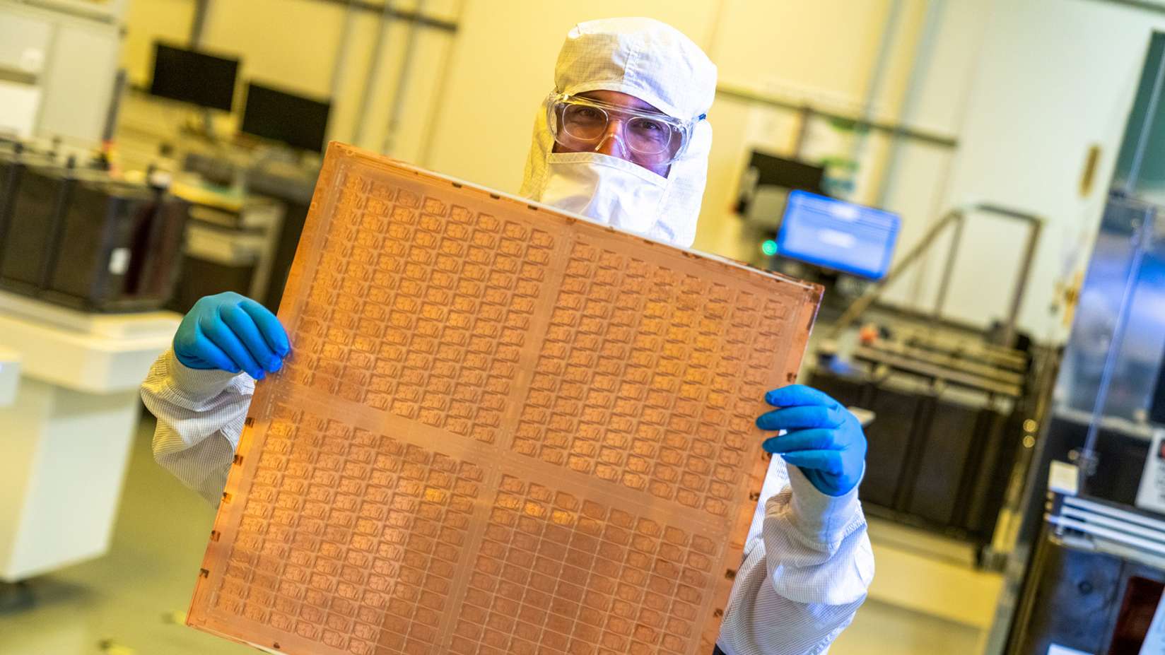
An Intel engineer holds a test glass core substrate panel at Intel’s Assembly and Test Technology Development factories in Chandler, Arizona, in July 2023. Intel’s advanced packaging technologies come to life at the company’s Assembly and Test Technology Development factories. (Credit: Intel Corporation)
Compared to today’s organic substrates, Intel said glass offered distinctive properties such as ultra-low flatness and better thermal and mechanical stability, resulting in much higher interconnect density in a substrate. These benefits allow chip architects to create high-density, high-performance chip packages for data-intensive workloads such as AI.
“Glass substrates can tolerate higher temperatures, offer 50% less pattern distortion, and have ultra-low flatness for improved depth of focus for lithography, and have the dimensional stability needed for extremely tight layer-to-layer interconnect overlay,” Intel said, adding that a 10x increase in interconnect density is possible on glass substrates.
Intel also noted that improved mechanical properties of glass enable ultra-large form-factor packages with very high assembly yields. The US chip giant is on track to deliver complete glass substrate solutions to the market in the second half of this decade, allowing the industry to continue advancing Moore’s Law beyond 2030.
“Glass substrates possess superior mechanical, physical and optical properties that allow for more transistors to be connected in a package, providing better scaling and enabling assembly of larger chiplet complexes (called “system-in-package”) compared to organic substrates in use today,” Intel added.
In short, chip architects can pack more tiles – chiplets – into a smaller footprint on one package while achieving performance and density gains with greater flexibility and lower overall cost and power usage.
“As the demand for more powerful computing increases and the semiconductor industry moves into the heterogeneous era that uses multiple “chiplets” in a package, improvements in signaling speed, power delivery, design rules, and stability of package substrates will be essential,” the chip giant noted.
Which industry will benefit first and most?
Intel believs that glass substrates will initially be introduced into the market where applications and workloads require larger form factor packages and higher speed capabilities. So, it will be more substantially used for data centers, AI, and graphics.
“Building on the momentum of recent PowerVia and RibbonFET breakthroughs, these industry-leading glass substrates for advanced packaging demonstrate Intel’s forward focus and vision for the next era of computing beyond the Intel 18A process node,” the chip giant said.
The company added that since it is on the path to delivering one trillion transistors on a package by 2030, the ongoing innovation in advanced packaging, including glass substrates, will help achieve this goal.


20 June 2024