Semiconductor: Siemens unveils software to test advanced packaging chips
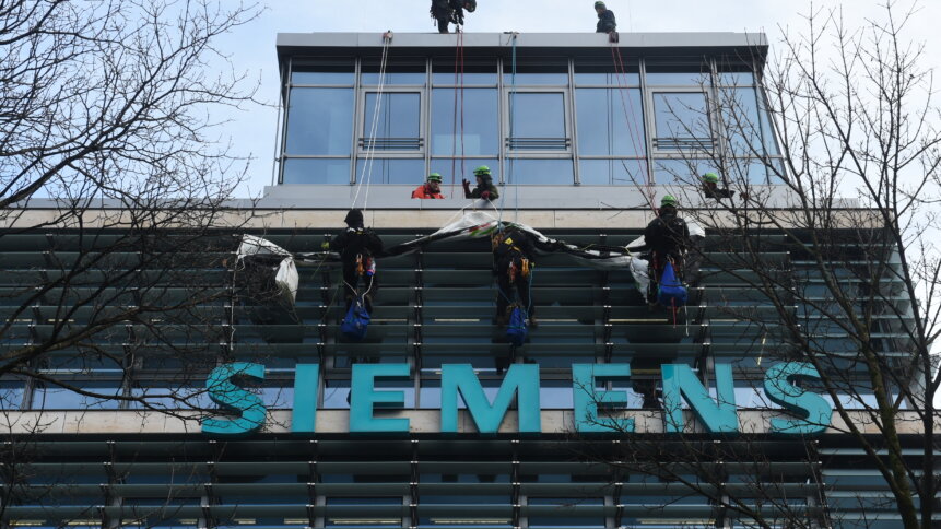
Semiconductor: Siemens unveils software to test advanced packaging chips. (Photo by Christof STACHE / AFP)
- Semiconductor chip testing processes have always been difficult and up till now, Siemens has had to work with customers on a case-by-case basis.
- Now, Siemens is automating the solution, making it available for everybody to use.
- Making the testing process easier for chips with advanced packaging, also referred to as 2.5 and 3-dimensional packaging, will boost the tech further.

Semiconductor chips have traditionally been packaged with only one silicon tile inside, but over the years, as the concept of “the smaller, the better” takes center stage, the industry has begun to face more challenges. After all, making features on chips smaller and smaller to cram more computing power into them is not an easy feat. Some chipakers even started stacking several features, sometimes mixing and matching different technologies, to improve performance.
But what happens after those chips are made? They will have to be tested, and that too comes as a challenge, as there are several layers of tiles. For Siemens Digital Industries Software, a unit of Germany’s Siemens that specializes in 3D & 2D Product Lifecycle Management software, the process of testing those chips is a meticulous one, done with customers on a case-by-case basis.
To overcome that hurdle, Siemens Digital Industries Software introduced a software, the Tessent™ Multi-die software solution, which helps customers dramatically speed up and simplify critical design-for-test (DFT) tasks for next-generation integrated circuits (ICs) based on 2.5D and 3D architectures. In simple terms, the software automates a design process for testing semiconductor chips made with advanced packaging.
For Siemens, demand for smaller, more power efficient and higher performing ICs continues to challenge the global IC design community. “Next-generation devices increasingly feature complex 2.5D and 3D architectures that connect dies vertically (3D IC) or side-by-side (2.5D) so that they behave as a single device. However, these approaches can present significant challenges for IC tests, since most legacy IC test approaches are based on conventional two-dimensional processes,” the company said.
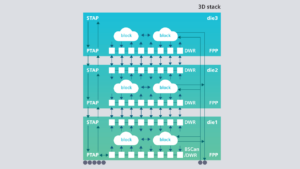
Siemens’ Tessent Multi-die software helps customers dramatically speed up and simplify critical design-for-test (DFT) tasks for next-generation integrated circuits (ICs) based on 2.5D and 3D architectures.
Considering that testing is a key part of the chip-making process, Siemens believes a port to test them has to be designed into the chip before they are made. Therefore, Siemens’ head of the Tessent business, Ankur Gupta, in a conversation with Reuters, said that Siemens was “taking all of those learnings and automating the solution, making it available for general purpose for everybody to use.” The end goal is to make the testing process easier for chips with advanced packaging, also referred to as 2.5 and 3-dimensional packaging, which Gupta explained will give the new technology a boost.

The new Tessent Multi-die solution works seamlessly with Siemens’ Tessent TestKompress Streaming Scan Network software and Tessent IJTAG software, which optimize DFT test resources for each block without concern for impacts to the rest of the design, thereby streamlining DFT planning and implementation for the 2.5D and 3D IC era.
“Using Tessent Multi-die software, IC design teams can rapidly generate IEEE 1838 compliant hardware featuring 2.5D and 3D IC architectures,” the company added. Separately, Pedestal Research’s President and Research Director Laurie Balch said that “More design teams are leveraging the power, performance and form factor advantages that 2.5D and 3D IC architectures can deliver, as the limits of traditional 2D IC design approaches become increasingly clear over time.”
But as Balch puts it, deploying these advanced schemes in new design starts without first establishing a DFT strategy that acknowledges the inherent challenges these architectures present can raise costs and undermine aggressive timelines. “However, by evolving DFT technology to keep pace with the rapid adoption of multi-dimensional designs, EDA vendors can play a key role in further enabling global, mainstream adoption of 2.5D and 3D architectures.”


20 June 2024