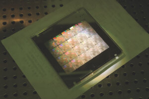
Nvidia claims breakthrough in chip manufacturing for 2nm and beyond

Nvidia claims breakthrough in chip manufacturing for 2nm and beyond. Pic: Nvidia
The annual Nvidia GPU Technology Conference (GTC) has just concluded, and the AI giant took the stage to unveil a new software library that will allow next-generation chips to be made at a faster rate with lower energy costs. Known as cuLitho, Nvidia spent four years developing the software on the company’s enterprise GPU hardware. It’s expected to revolutionize Nvidia chip design.
The breakthrough accelerates the field of computational lithography, enabling industry leaders to accelerate the design and manufacturing of 2nm chips and beyond. Computational lithography is the process of etching the components of a processor into a silicon wafer. Because the demand for smaller manufacturing processes has increased, lithography has gotten more complex, and the current technology has reached an inflection point.
cuLitho also reduces chip fab data center carbon footprint and can push the boundaries of bleeding-edge semiconductor design. So far, Nvidia cuLitho has already been adopted by the world’s top chip foundry, TSMC, leading EDA chip design tools company Synopsys and chip manufacturing equipment maker ASML.
“With lithography at the limits of physics, Nvidia’s introduction of cuLitho and collaboration with our partners TSMC, ASML, and Synopsys allows fabs to increase throughput, reduce their carbon footprint and set the foundation for 2nm and beyond,” Jensen Huang, founder, and CEO of Nvidia said in his keynote address at the annual GTC developer conference.
How does Nvidia cuLitho accelerate chip manufacturing?
Known as cuLitho, Nvidia had spent four years developing the software which runs on the company’s enterprise GPU hardware.
Source: Nvidia
To appreciate the significance of the development, it is necessary to understand how the cost of the computational time needed for the largest workloads in semi-manufacturing has, in recent years, been outpacing Moore’s law, due to both the more significant number of transistors in newer nodes and more stringent accuracy requirements. “Future nodes require more detailed calculations, not all of which can feasibly fit into the available computational bandwidth provided by the current platforms, slowing the pace of innovation in semiconductors. A fab process change often requires an OPC revision, creating bottlenecks,” Nvidia explained in a statement.
That is when cuLitho comes in, and it will not only help to remove these bottlenecks but also make possible novel solutions and innovative techniques like curvilinear masks, high NA EUV lithography, and sub-atomic photoresist modeling needed for new technology nodes, Nvidia noted.
Running on GPUs, or graphics processing units, cuLitho delivers a performance leap of up to 40x beyond current lithography — creating patterns on a silicon wafer — accelerating the massive computational workloads that currently consume tens of billions of CPU hours every year, Nvidia said.
YOU MIGHT LIKE

NVIDIA brings a world of AI innovation to enterprise
It also enables 500 NVIDIA DGX H100 systems to achieve the work of 40,000 CPU systems, running all parts of the computational lithography process in parallel, helping reduce power needs and potential environmental impact. “In the near term, fabs using cuLitho could help produce 3-5x more photomasks each day — the templates for a chip’s design — using 9x less power than current configurations,” the AI giant said.
Essentially, using cuLitho, a photomask that requires two weeks can be processed overnight. Even more interesting is that cuLitho will enable better design rules, higher density, higher yields, and AI-powered lithography in the long term.
“Originally, photomasks were just a negative of the shape engineers were trying to etch into the silicon, but as transistors have gotten smaller, these photomasks became more complex to counteract the effects of optical distortion,” an article by The Register reads.
If unchecked, this distortion can blur these features beyond recognition. “This process is called optical proximity correction (OPC) and more recently has evolved into inverse lithography technology (ILT). In the case of the latter, the photomasks look nothing like the feature they’re designed to print,” the article stated.
That means the more ornate these photomasks get, the more computational horsepower is required to produce them. On the other hand, Nvidia believes that using GPUs can speed up this process and reduce the power needed.
“It’ll help the semiconductor industry continue the pace of innovation that we’ve all come to rely on, and it’ll improve the time to market for all kinds of chips in the future,” Vivek Singh, VP of Nvidia’s advanced technology group, explained during a press conference on Monday.


20 June 2024