Photonic chips could lighten AI’s carbon footprint
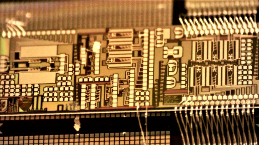
Circuit training: photonic processors pave the way for more efficient on-chip training of neural networks. Image credit: The George Washington University/Queens University.
Training vast amounts of data using deep learning algorithms can produce fascinating results. Examples include Generative Pre-trained Transformer 3 (better known as GPT-3) – currently, the world’s most powerful auto-regressive language model. But the computational budget (and energy overhead) required by these huge artificial intelligence (AI) undertakings has prompted concerns over AI’s carbon footprint.

To be clear, the benefits of AI are huge. GPT-3 can be thought of as text auto-complete on steroids. Fed with plain language, the deep learning model can turn those human-readable instructions into computer code. It’s a productivity-boosting feature that Microsoft, which has licensed GPT-3 from developer OpenAI, is using in its so-called ‘Power Apps’. By leveraging AI, the software allows users to achieve computer programming results with little or no coding experience.
Time and money
Earlier this year, OpenAI announced new GPT-3 capabilities that enable not just the ability to complete an unfinished sentence, but also make it practical for the model to rewrite an existing paragraph or refactor lines of code. But getting to this point has required a great deal of processing power. GPT-3’s 175 billion parameter model, reportedly required 3.14E23 FLOPS of computing for training.
Chuan Li of Lambda Labs – a provider of cloud services – writes that even at a theoretical 28 TFLOPS for an NVIDIA Tesla V100 cloud instance and the lowest three-year reserved cloud pricing that his team could find, a single training run will take 355 GPU-years and cost around $4.6 million. It highlights the kind of ballpark figures required for state-of-the-art deep learning models and brings us back to concerns over AI’s carbon footprint, given the power demands of GPUs.

With the COP27 climate conference fresh in people’s minds, energy-intensive operations are again coming under scrutiny. Powering cloud computing with clean energy is one answer, but this needs to be coordinated to ensure that processing coincides with the availability of renewable electricity. And even this scenario doesn’t address all the concerns.
Photonic integrated circuits
There’s also the issue of high costs limiting the development of these kinds of massive AI models to just a handful of companies with big financial pockets. Fortunately, an up and coming type of computing architecture could change things on multiple fronts – one that leverages not just electrons, but photons too.
Over the past decade, chip designers have made great progress in the realm of silicon photonics, which taps into the fabrication advances of silicon-based integrated circuits to engineer a range of light-based operations. Photonic integrated circuits (PICs) offer low-latency, high-bandwidth, and inherently parallel processing (using optical multiplexing).
Previously, PICs have been shown to be capable of performing inference (inferring features from new data using an existing algorithm). But the AI model itself still had to be trained offline in a conventional, and energy-intensive, way. But now, researchers in the US and Canada have come up with a PIC concept that can do both – reporting their results in the latest issue of the journal Optica (open access article).

The team believes that its novel hardware will speed up the training of machine learning systems and harness the best of what both photonics and electronic chips have to offer. The group has been working hard on building photonic versions of tensor cores (processors that outperform GPUs in completing standard AI-related operations). And this latest breakthrough is part of that larger effort.
Low-power consumption photonics with high bandwidth information processing characteristics are, on paper, well suited to reducing AI’s carbon footprint. But when it comes to training deep learning models, the ‘back propagation step’ – where model weights are adjusted to generalize features exhibited by the data more accurately – has slowed things down. Network layers must be updated sequentially.
Multi-channel improvements
To get around this, the researchers have taken another approach known as direct feedback alignment (DFA) that allows the network to be updated in parallel. “During the backward pass, the error from the network’s inference step is encoded on multi-channel optical inputs,” explain the authors in their paper. “The electro-optic circuit then calculates the gradient vector for each hidden layer, which is used to update the network parameters stored in memory using an external digital control system.”
Another potential hurdle when using PICs rather than purely digital electronics is the noise that’s inherent to analog circuits. However, neural networks turn out to be robust to noise (one of the reasons for their broad success) during both inference and training. Also, thanks to DFA, noise doesn’t accumulate between network layers, which would otherwise be the case. During backpropagation, errors are stepped from the output through each of the hidden layers (the inner workings of the AI algorithm) as part of the training process.
“The training of AI systems costs a significant amount of energy and carbon footprint,” emphasizes Volker Sorger of George Washington University, one of the institutions that took part in the study. “For example, a single AI transformer takes about five times as much CO2 in electricity as a gasoline car spends in its lifetime.” And the team, which includes researchers from Queens University, University of British Columbia, and Princeton University, hopes that training on photonic chips will help to reduce this overhead.
To explore the opportunities of photonic technology in a commercial setting, Sorger has founded a start-up company dubbed Optelligence, together with Hamed Dalir. The firm has its headquarters in Austin, Texas, and a manufacturing facility located in Ashburn, Virginia.
5 March 2024